- 您现在的位置:买卖IC网 > Sheet目录478 > MMA8452QR1 (Freescale Semiconductor)IC ACCELER 2G/4G/8G 3AXIS 16QFN
2.3
I 2 C interface characteristics
Table 4. I 2 C slave timing values (1)
Parameter
Symbol
I 2 C Fast Mode
Min Max
Unit
SCL clock frequency
Bus-free time between STOP and START condition
(Repeated) START hold time
Repeated START setup time
STOP condition setup time
f SCL
t BUF
t HD;STA
t SU;STA
t SU;STO
0
1.3
0.6
0.6
0.6
400
kHz
μ s
μ s
μ s
μ s
SDA data hold time
SDA setup time
SCL clock low time
SCL clock high time
t HD;DAT
t SU;DAT
t LOW
t HIGH
0.05
100
1.3
0.6
0.9
(2)
μ s
ns
μ s
μ s
SDA and SCL rise time
SDA and SCL fall time
(4)
SDA valid time
SDA valid acknowledge time (5)
Pulse width of spikes on SDA and SCL that must be suppressed by
internal input filter
Capacitive load for each bus line
t r
t f
t VD;DAT
t VD;ACK
t SP
Cb
20 + 0.1 C b
20 + 0.1 C b
0
(3)
(3)
300
300
0.9 (2)
0.9 (2)
50
400
ns
ns
μ s
μ s
ns
pF
1.All values referred to V IH(min) (0.3V DD ) and V IL(max) (0.7V DD ) levels.
2.This device does not stretch the LOW period (t LOW ) of the SCL signal.
3.C b = total capacitance of one bus line in pF.
4.t VD;DAT = time for data signal from SCL LOW to SDA output (HIGH or LOW, depending on which one is worse).
5.t VD;ACK = time for Acknowledgement signal from SCL LOW to SDA output (HIGH or LOW, depending on which one is worse).
V IL = 0.3V DD
V IH = 0.7V DD
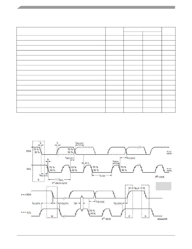
Figure 5. I 2 C slave timing diagram
MMA8452Q
Sensors
8
Freescale Semiconductor, Inc.
发布紧急采购,3分钟左右您将得到回复。
相关PDF资料
MMA8453QR1
IC ACCELER 2G/4G/8G 3AXIS 16QFN
MMBF0201NLT1
MOSFET N-CH 20V 300MA SOT-23
MMBF170-7
MOSFET N-CH 60V 500MA SOT23-3
MMBF170LT1
MOSFET N-CH 60V 500MA SOT-23
MMBF170
MOSFET N-CH 60V 500MA SOT-23
MMBF2201NT1
MOSFET N-CH 20V 300MA SOT-323
MMBF2202PT1
MOSFET P-CH 20V 300MA SOT-323
MMDF1N05ER2G
MOSFET N-CHAN DUAL 2A 50V 8SOIC
相关代理商/技术参数
MMA8452QT
功能描述:加速计 - 板上安装 LOW G 3-AXIS 12BT EX VLT
RoHS:否 制造商:Murata 传感轴:Double 加速:12 g 灵敏度: 封装 / 箱体: 输出类型:Analog 数字输出 - 位数:11 bit 电源电压-最大:5.25 V 电源电压-最小:4.75 V 电源电流:4 mA 最大工作温度:+ 125 C 最小工作温度:- 40 C
MMA8453Q
制造商:FREESCALE 制造商全称:Freescale Semiconductor, Inc 功能描述:Xtrinsic MMA8453Q 3-Axis, 10-bit/8-bit Digital Accelerometer
MMA8453QR1
功能描述:加速计 - 板上安装 LOW G 3-AXIS DGTL ACCEL
RoHS:否 制造商:Murata 传感轴:Double 加速:12 g 灵敏度: 封装 / 箱体: 输出类型:Analog 数字输出 - 位数:11 bit 电源电压-最大:5.25 V 电源电压-最小:4.75 V 电源电流:4 mA 最大工作温度:+ 125 C 最小工作温度:- 40 C
MMA8453QT
功能描述:加速计 - 板上安装 LOW G 3-AXIS DGTL ACCEL
RoHS:否 制造商:Murata 传感轴:Double 加速:12 g 灵敏度: 封装 / 箱体: 输出类型:Analog 数字输出 - 位数:11 bit 电源电压-最大:5.25 V 电源电压-最小:4.75 V 电源电流:4 mA 最大工作温度:+ 125 C 最小工作温度:- 40 C
MMA8491Q
制造商:FREESCALE 制造商全称:Freescale Semiconductor, Inc 功能描述:Xtrinsic MMA8491Q 3-Axis Multifunction Digital Accelerometer
MMA8491QR1
功能描述:加速计 - 板上安装 3-Axis Low Voltage Discrete Tilt Sensor
RoHS:否 制造商:Murata 传感轴:Double 加速:12 g 灵敏度: 封装 / 箱体: 输出类型:Analog 数字输出 - 位数:11 bit 电源电压-最大:5.25 V 电源电压-最小:4.75 V 电源电流:4 mA 最大工作温度:+ 125 C 最小工作温度:- 40 C
MMA8491QT
功能描述:加速计 - 板上安装 3-Axis Low Voltage Discrete Tilt Sensor
RoHS:否 制造商:Murata 传感轴:Double 加速:12 g 灵敏度: 封装 / 箱体: 输出类型:Analog 数字输出 - 位数:11 bit 电源电压-最大:5.25 V 电源电压-最小:4.75 V 电源电流:4 mA 最大工作温度:+ 125 C 最小工作温度:- 40 C
MMA8652FC
制造商:FREESCALE 制造商全称:Freescale Semiconductor, Inc 功能描述:Xtrinsic MMA8652FC 3-Axis, 12-bit Digital Accelerometer
